VLSI Design Laboratory
VLSI Design Laboratory
Lab Overview
Introduction
The VLSI Design Laboratory at the Department of Electronics & Communication Engineering is a state-of-the-art facility equipped with cutting-edge FPGA development platforms and industry-standard EDA tools. With a seating capacity of 36 students and dedicated server support, the lab provides a comprehensive environment for hands-on learning, innovative project development, and advanced research in digital and VLSI system design.
The laboratory serves as a key enabler for undergraduate and doctoral students to build, simulate, prototype, and test custom digital hardware systems, fostering innovation and industry-ready skill development.
Mission / Vision
The lab aims to cultivate a deep understanding of Digital Systems with FPGA, VLSI Design, and VLSI architecture. Its mission is to empower students and researchers to innovate in hardware design and full-custom VLSI, contribute to industry-relevant solutions, and advance knowledge in energy-efficient computation and next-generation communication architectures.
Focus Areas
- Design of reliability-aware neuromorphic computing architectures
- In-memory computing architectures for machine learning applications
- FPGA-based system design and prototyping
- VLSI architectures for signal processing and communication
- Hardware accelerators for AI/ML and DSP
- ASIC implementation for energy-efficient and real-time systems
- Satellite communication and digital beamforming architectures
- MEMS devices including FBAR/BAW RF resonators, pressure sensors, and accelerometers
Laboratory Facilities
Computing Infrastructure
- 36 high-performance workstations (Intel i5/i7, 8–16 GB RAM, Windows/Linux)
- 1 high-end server (Intel Xeon, 64 GB RAM, Linux)
EDA Tools and Software
- Xilinx Tools: Xilinx System Edition (25 perpetual licenses – SNU)
- AMD/Xilinx: Vivado & Vitis (50 licenses – C2S, CDAC)
- Synopsys Suite: Design Compiler, IC Compiler II, PrimeTime, VCS, Fusion Compiler
- Cadence Suite: Virtuoso, Spectre, Innovus, Genus, Tempus
- MEMS Design Tools: CoventorWare, COMSOL Multiphysics
FPGA Development Boards
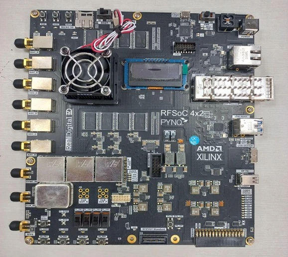
- AMD/Xilinx RFSoC 4x2 Board – 1
- AMD/Xilinx Pynq-Z2 Board – 1
- Nexys-4 (Artix-7) Boards – 12
- Nexys-A7 (Artix-7) Boards – 8
PMOD Extension Modules
- Dual H-Bridge, Digital Potentiometers, Slide Switches
- Temperature & Humidity Sensors
- WiFi, Bluetooth, Zigbee Modules
- 16-Hex Keypad, OLED RGB Display
Research and Innovation
Publications
- V. Singh et al., Diversity Combining Scheme for Time-Varying STBC NGSO Multi-Satellite Systems, IEEE Communications Letters, 2024.
- J. B. Shaik et al., Impact of Aging and Process Variability on SRAM-Based In-Memory Computing Architectures, IEEE TCAS-I, 2024.
- J. B. Shaik et al., Reliability-aware design of Integrate-and-Fire silicon neurons, Integration, 2024.
- Megha Nawaria et al., Memristor-inspired Digital Logic Circuits, IEEE TED, 2024.
- S. M. Picardo et al., Reliability-aware neuromorphic circuit design, IJCTA, 2022.
- Additional publications spanning neuromorphic circuits, SRAM reliability, satellite communications, and MEMS devices.
Collaborations
- Shanghai Jiao Tong University Joint Institute, China
- BITS Pilani – Dubai Campus
- University of Luxembourg
Innovation Corner
- Reliability-aware CMOS circuits for neuromorphic systems
- Extreme Learning Machine hardware models
- 5-stage pipelined RISC-V processor implementation on FPGA
Academic Integration
Courses Supported
- VLSI Design (Elective)
- Digital Design with FPGAs (Elective)
- Reconfigurable Computing (Elective)
Hands-On Learning
- Computing-in-memory architecture for CNNs
- Reliability analysis of MAC units
- FPGA-based AI-powered drone
- RISC-V processor and fault-tolerant architectures
- Hardware accelerators for cryptography and matrix multiplication
Workshops & Training
- FPGA/SoC Demonstration and Training – February 2025
- Expert Talk on FPGA-Based Accelerated IoT Edge Computing – February 2025
- Expert Talk on CMOS Design Challenges – February 2024
- Upcoming FDP: RTL to GDSII Flow for ASIC Design – July 2025
Industry Collaboration
- Industry-sponsored initiatives under Chip to Startup (C2S) Program
- Internship and project collaboration with Cadence Design Systems
Lab Safety & Guidelines
Protocols
- Lab access only under faculty or lab staff supervision
- Strict adherence to ESD and electrical safety guidelines
- Preventive maintenance and controlled equipment usage
Training
- Mandatory lab safety induction every semester
- Regular fire safety and emergency response training
Contact
Prof. Sonal Singhal
Dr. Rakesh Palisetty
Mr. Mohan Kumar
News & Events
Recent Updates
- Received AMD/Xilinx Vivado and Vitis licenses under the C2S Program
- Received full Synopsys EDA tool suite for ASIC design and verification