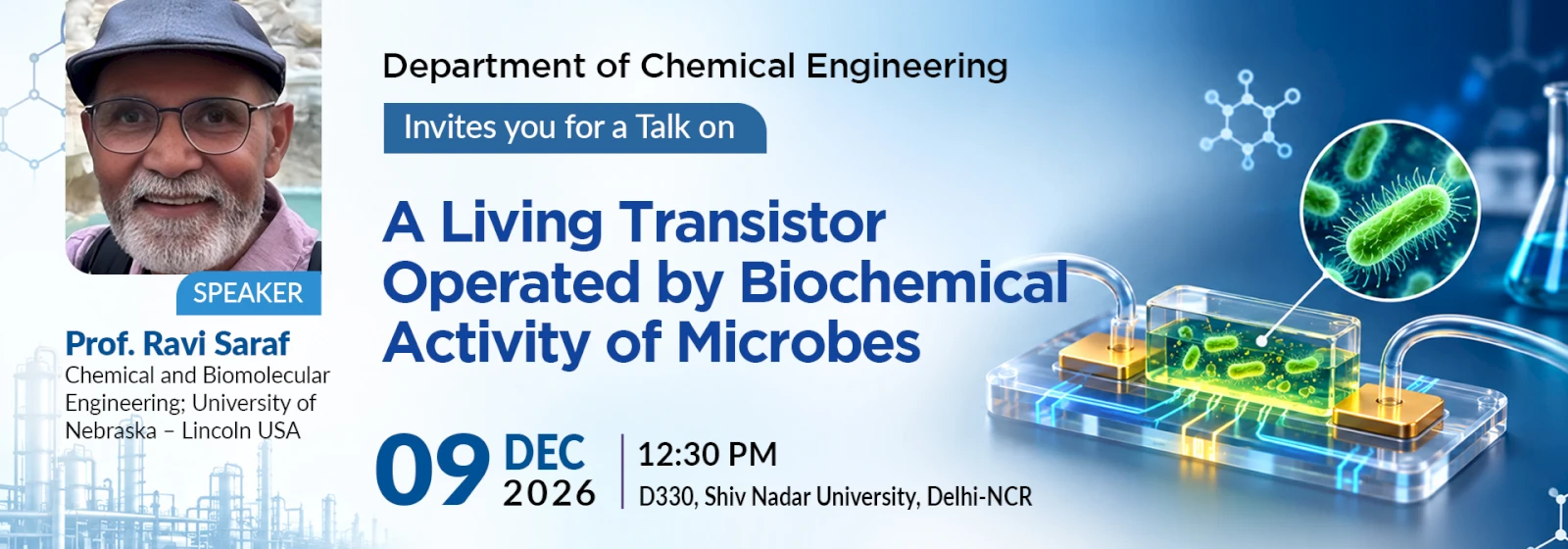
A Living Transistor Operated by Biochemical Activity of Microbes
Abstract
The spontaneous formation of sub-nanometer scale electrical double layer (EDL) makes water an ideal media to make transistors. The EDL is more than two-fold thinner with 10-fold higher dielectric constant than modern day “gate-oxides” used in electronic chips. However, the performance to gate a semiconductor transistor-channel degrades due to the strong interaction with high charge density in EDL. Noble metals are ideal because they are inert and form a stable and uniform EDL. Unfortunately, unlike semiconductors, metal do not have a conduction gap required to make transistor channels that can be gated. Thus, it is impossible to make a metallic transistor with high performance. (Although, low performance metal transistor have been developed with switching gain of 2-100 fold under extreme conditions). A novel principle of an electrochemical field effect transistor (eFET) made from noble metal operating in water is developed. The transistor channel is made of a special two dimensional (2D) network of self-assembled one dimensional (1D) necklaces of 10 nm Au particles. These nanoparticle necklace network (N3) exhibit a strong conduction gap that can be tailored from 0 V (metallic) to 5.5 V. The conduction gap can be tuned by gating the channel via the EDL to obtain a switching gain of 104-fold. Leveraging the high gain and facile interface with metallic channel with naturally nano-rough interface, a “living transistor” gated by biochemical activity of microorganisms is made. Living transistors gated by high electrical activity mammalian cells (such as neurons, heart and muscle cells) have been shown using semiconducting materials (made from graphene, CNT, and nanowires), microbes have been a challenge due to their thick cell wall. The low power and small format of these eFET microsensor has potential applications in combinatorial synthetic biology, and medical application such as sepsis and antibiotic resistance.
I will start the discussion with the basics of a transistor, describe an electrochemical transistor, leading the discussion to fabrication and performance of our N3-eFET. I will discuss the physics, engineering, and bio-application of our living transistor at level understandable by advanced undergraduate and graduate level students.
Brief Profile:
Ravi Saraf is Lowell E & Betty Anderson Professor of Chemical and Biomolecular Engineering at the University of Nebraska – Lincoln (UNL). After his BTech in Chemical Engineering from IIT, Kanpur he joined the group of Professor Roger Porter at the University of Massachusetts – Amherst to pursue PhD in Polymer Science and Engineering. From Amherst, he joined the IBM’s prestigious T.J. Watson Research Center at Yorktown, NY conducting research on microelectronics fabrication, packaging and devices. After spending 12 years at IBM, in 2004 he moved to academia, first at Virginia Tech for 5 years then subsequently as a chaired professor at UNL, his current position. Saraf has over 55 issued US Patents and well over 120 peer reviewed publications in nanomaterials, polymer, microelectronics, electrochemistry, measurement science, and device physics. His quantum mechanical tactile device to image texture at resolution of human finger was featured in numerous magazines and news outlets, and in 2009 was chosen as top 100 inventions by Discovery magazine. It was featured in the compilation of inventions by science editors of The Times, UK. His team built the first electrochemical field effect transistor operating in water that was featured in Nature. His broad area of research is in nanotechnology using exotic nanomaterials, novel device physics and measurement science. His primary research is translational where fundamental science is applied to solving practical problems. Saraf has founded a company, Vajra Instruments, Inc to develop electronic and opto-electronic devices.
Share this: